


I recently moderated a panel at Deep Tech Week with three people who know far more about optical interconnects than most of us should reasonably be expected to know: Dr. Julie Sheridan Eng, CTO of Coherent; Dr. Matthew Sysak, CTO of Lumentum; and Ramin Farjadrad, CEO of Eliyan.
I warned the audience that this would be a major geek-out session. I believe we delivered.
My starting position was intentionally provocative: the primary limitation in large AI systems is no longer only the speed of the processor. It is increasingly the interconnect.
A modern AI cluster distributes work across hundreds or thousands of processors. These devices must continually exchange model parameters, intermediate results, and memory contents. A faster GPU has limited value if it spends too much time waiting for data from another GPU.
This makes the interconnect part of the computer rather than simply a cable between computers.
You can check out our full conversation or some of the main insights from the panelists summarized below. Thanks for reading.
There is no single optical interconnect
The first point worth clarifying is that “AI optics” is not one application.
The industry now talks about scale-in, scale-up, scale-out, and scale-across networks:
Scale-in connects individual die or chiplets within a package.
Scale-up connects processors within a rack or a tightly coupled group of racks.
Scale-out connects racks throughout a data center.
Scale-across connects data centers over much longer distances.
Each has a different set of requirements.
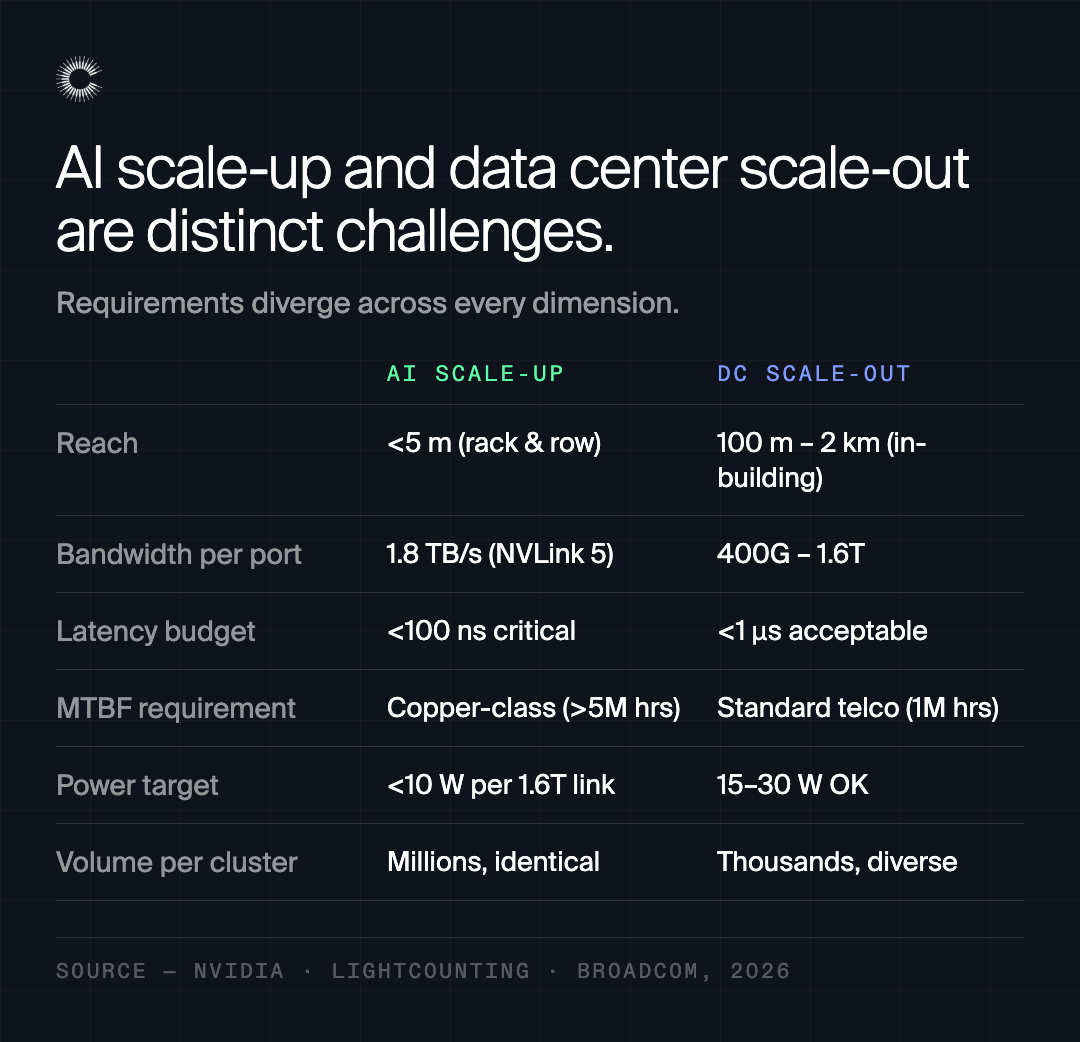
For a connection spanning hundreds of kilometers, the cost of fiber and the number of wavelengths carried on each fiber matter greatly. An additional few watts or nanoseconds may be acceptable.
Inside a rack, the calculation changes. The distance may be only a few meters, but the number of connections is enormous. Power, latency, density, reliability, and cost per link become more important than maximizing the number of bits carried on each fiber.
This is why several optical technologies continue to coexist. Indium phosphide, silicon photonics, gallium arsenide VCSELs, coherent optics, active copper, linear pluggable optics, and co-packaged optics each have useful characteristics. There is no reason to expect one technology to replace all the others.
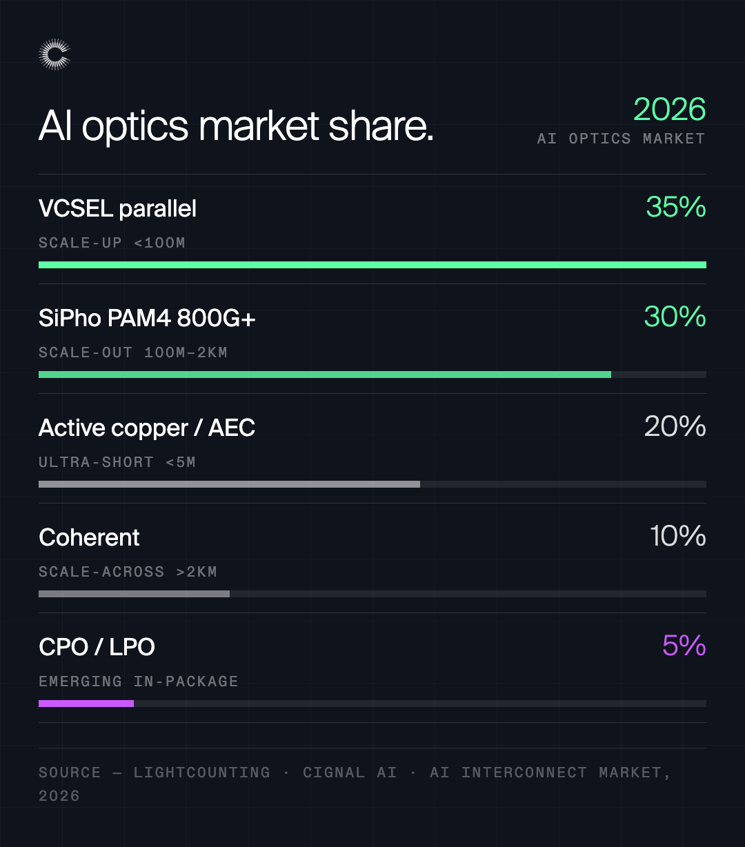
The correct question is not “Which optical technology wins?” It is “Which technology best fits the reach, bandwidth, power, latency, reliability, and manufacturing requirements of the application?”
Scale-up is the difficult part
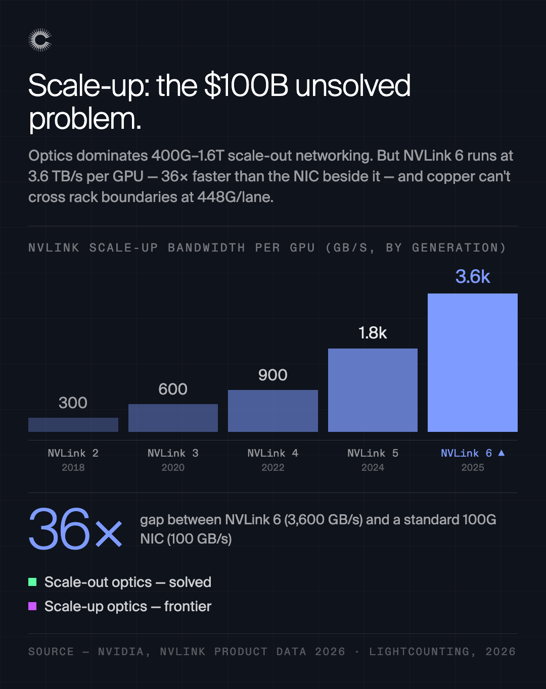
Optics is already well established in scale-out networks. Moving data between racks at 400G, 800G, and 1.6T is a real engineering challenge, but the basic technologies and supply chains exist.
Scale-up presents a different problem.
The panel slides compared NVLink 6 bandwidth of 3.6 terabytes per second per GPU with a standard 100-gigabyte-per-second network interface. That is a 36-times difference. At the same time, copper has difficulty extending across rack boundaries as lane rates approach 448 gigabits per second.
Copper has served the industry well because it is reliable, inexpensive, familiar, and readily available. Engineers do not abandon those advantages casually.
Unfortunately, physics is not very sentimental.
As electrical signaling rates increase, reach decreases. More equalization and signal processing can extend the distance, but those techniques consume power and add complexity. Eventually, the electrical link costs too much power, occupies too much space, or cannot reach the next processor.
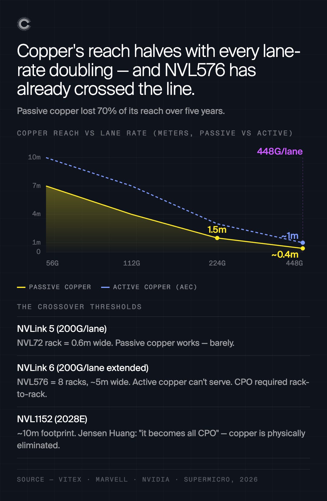
Optics can extend the reach and improve density, but it must approach copper-class reliability and power consumption before it can be used deeply inside the compute system.
That is a considerably harder requirement than building a pluggable optical module for the front of a network switch.
Faster lanes are not free
The optical industry has historically increased bandwidth by raising the data rate of each lane and then adding more lanes when further increases became difficult.
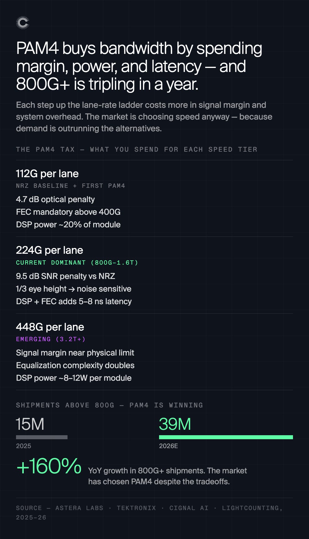
PAM4 encoding has been very effective in this process. It carries two bits per symbol using four signal levels rather than the two levels used by NRZ. The trade-off is that the signal levels are closer together and therefore more sensitive to noise.
Higher PAM4 rates require more sophisticated digital signal processors, forward error correction, and equalization. These improve the link, but they consume power and can add latency.
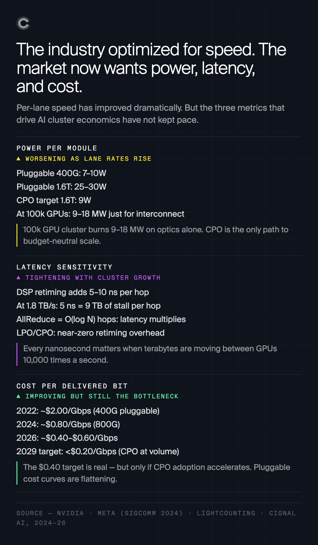
At 224 gigabits per second per lane, the panel materials estimated that DSP and error correction can add five to eight nanoseconds of latency. That may sound small. In a tightly coupled system performing repeated communication across many hops, it is not small.
There are two basic architectural choices.
One approach uses fewer lanes running at very high speeds. This reduces the number of fibers and optical components but requires more complex electronics.
The other uses more lanes at lower speeds. This increases the fiber and packaging count but can reduce DSP power, latency, and signal-processing complexity.
For long-distance links, fewer and faster lanes usually make sense. Nobody wants to run 100 fibers across ten kilometers if ten fibers will do the job.
For scale-up and scale-in, “slow and wide” becomes more attractive. Fiber count is less important, while latency, power, redundancy, and reliability are critical. This is one reason NRZ is receiving renewed attention for short-reach optical systems.
Sometimes progress means using a simpler modulation format and a lot more wires.
Reliability becomes a system-level problem
Optics must also scale in manufacturing volume and reliability.
Julie made an important observation. At 10G, the industry had approximately 15 years to produce its first ten million units. At current rates, it may have only four years.
The physical problems are becoming harder at the same time that manufacturing schedules are becoming shorter.
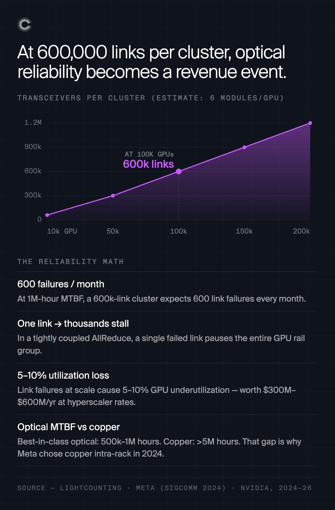
A large cluster may contain hundreds of thousands of optical links. At that scale, even a low component failure rate becomes visible at the system level. One failed link can stall many processors, reduce cluster utilization, and interrupt a workload that is consuming a considerable amount of electricity.
The panel materials modeled a cluster with 600,000 links and approximately 600 link failures per month, potentially contributing to a 5 to 10 percent utilization loss. The exact number will vary by architecture, but the point is valid: optical reliability can directly affect revenue.
Power has the same scaling effect. Removing a DSP may save only a few watts per module. Across a 100,000-GPU cluster, the panel estimated savings of approximately nine megawatts.
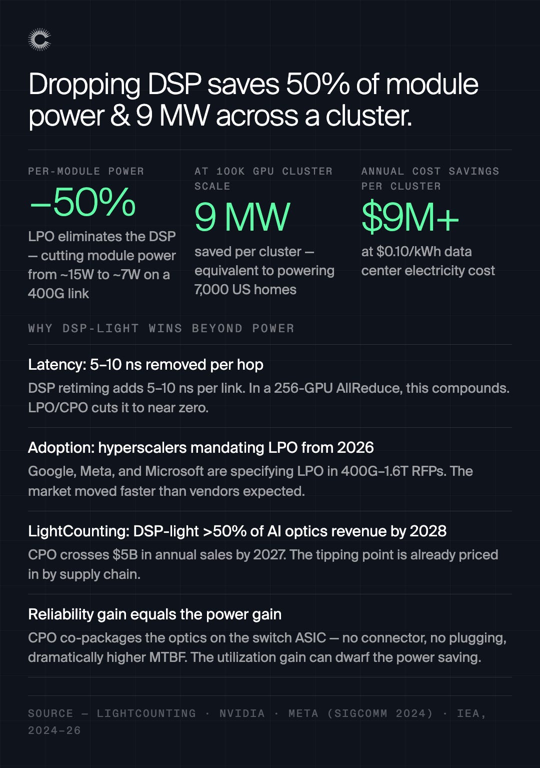
Small component improvements are no longer small when repeated hundreds of thousands of times.
Different devices will serve different distances
We also discussed several device technologies being considered for shorter optical links.
MicroLEDs offer extremely high emitter density. They may be useful for very short connections, although their low optical power and lack of directionality limit their reach.
VCSELs are already manufactured at large scale for applications such as smartphone sensing. They are attractive for links spanning a few meters because the technology is mature, dense, and relatively inexpensive.
Silicon photonics becomes more attractive over longer distances because it can place substantial bandwidth on a small number of fibers and make use of an established laser ecosystem.
These technologies are not necessarily direct substitutes. Their useful ranges overlap, but each has different strengths. My opinion is that the scale-up market will support multiple approaches because the architectures themselves are still changing.
Optical circuit switching has practical value
Optical circuit switching was another interesting topic.
The original use case was often described as replacing an electronic spine switch. In practice, one of its most useful functions may be reconfiguring the physical connections between processors.
A cluster optimized to train one large model may need a different topology when running many smaller inference workloads. An optical circuit switch can change those connections through software rather than requiring technicians to recable the system.
It can also route around a failed rack or bring backup capacity online.
This is not packet switching. The optical circuit switch does not inspect and route each packet. It changes the physical path through which the packets travel.
The distinction matters, and so does the benefit. Expensive processors are useful only when they are operating.
What should startups work on?
We ended by asking where new companies should focus through 2030.
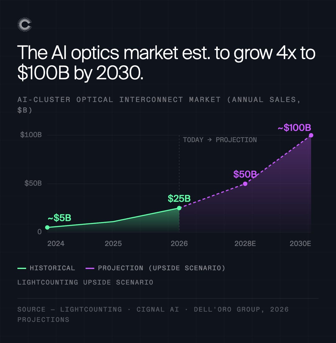
The answers included scale-in optics, die-to-die communication, new packaging techniques, thermal materials, optical circuit switching, and quantum networking.
The more important advice was simpler: start with the problem, not the technology.
A technically impressive device is not a company until someone has a reason to deploy it. Founders need to identify the specific bottleneck, explain why existing systems cannot solve it, and understand which partners are required to manufacture and deliver the product.
Hardware startups already carry considerable execution risk. Adding uncertain demand, an unclear application, and an unproven supply chain at the same time is generally not advisable. Try to keep the major risk concentrated in one place.
I closed the panel by recalling the old statement that software was eating the world.
My slightly biased view is that hardware is now eating software.
At a minimum, software is discovering that it still has to obey bandwidth, power, latency, heat, and the speed of light.
Dr. Steve Fu is a Partner at Celesta Capital, a deep tech venture capital firm investing across semiconductors, AI infrastructure, and connectivity. Before Celesta, he was Chief Strategy Officer at Fairchild Semiconductor, where he led R&D, new business incubation, partnerships, and acquisitions. He holds a PhD in Electrical Engineering from Stanford University and a BSEE from UC Berkeley.